I. Introduction
In the modern world of technology that surrounds us, tiny electronic chips have become an essential part of our daily lives. Whether it's our smartphones, computers, or various electronic devices, their interiors hide small yet powerful electronic components that play a crucial role in semiconductor manufacturing. However, to create these tiny and intricate electronic components, a highly precise process is required – lithography technology.
Lithography technology, although perhaps not well-known to most people, is a vital pillar of modern technology and the electronics industry. It is a complex and precise process used to accurately transfer microscopic circuit patterns onto semiconductor materials, thus producing powerful microprocessors, memory chips, sensors, and other semiconductor devices. Additionally, lithography technology also plays a critical role in photonics, optoelectronics, nanotechnology, biomedical sciences, and many other fields.
This article delves into the core concepts, historical development, technological advancements, application areas, and future trends of lithography technology. We will discover that lithography is not just a manufacturing technique; it is a driving force behind our modern way of life, providing a solid foundation for the continuous evolution of electronic devices. In this article, we will explore the mysteries of lithography technology and understand how it shapes the world of micro and nanostructures.
II. Basic Concepts
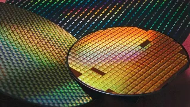
The core concept of photolithography is to transfer the precise pattern onto the photosensitive layer on the surface of a silicon wafer through optical projection, and then create the desired micro-pattern on the wafer through chemical processing. In this section, we will explain in detail the basic principles and steps of photolithography, as well as the main functions and components of photolithography machines.
2.1 Basic Principles
The basic principles of photolithography involve the following key concepts:
Photomask: One of the important elements that controls the final pattern. The photomask is a flat glass or quartz plate with a pattern that is blocked or transmitted through the photoresist during photolithography. This pattern is created using computer-aided design (CAD) software and is used for projection in photolithography.
Light source: One of the key parts of the photolithography machine. Usually, ultraviolet (UV) light sources are used because of their shorter wavelength, which enables higher resolution. The UV light source is irradiated onto the photomask and then the pattern is projected onto the surface of the silicon wafer through a series of lenses and reflectors.
Photosensitive layer: The goal of photolithography is to replicate the pattern on the photomask onto the silicon wafer. To achieve this, the silicon wafer needs to be covered with a layer of photosensitive material, typically photoresist. The photosensitive layer can be chemically altered by the irradiation of the light source on the photolithography machine.
2.2 Steps of Photolithography
The steps of photolithography usually include the following:
Wafer preparation: First, the silicon wafer is prepared, typically through chemical cleaning and other pre-treatment steps, to ensure the success of photolithography.
Photoresist coating: The photoresist is evenly coated on the surface of the silicon wafer. The photoresist is part of the photosensitive layer and is used to receive the projection of light and undergo chemical reactions in subsequent steps.
Mask alignment: The photolithography machine ensures that the mask and the silicon wafer are aligned so that the pattern can be accurately projected onto the silicon wafer.
Light projection: The light source projects the pattern on the photomask precisely onto the photosensitive layer. The photosensitive layer undergoes a chemical reaction under the irradiation of light, and its properties change.
Photoresist development: Next, the silicon wafer is placed into a special solution called the developing solution. The developing solution removes the photoresist that has not been irradiated by light, leaving only the irradiated part to form the desired pattern.
Post-processing: Depending on specific application requirements, the silicon wafer may need further chemical or physical processing steps, such as etching, ion implantation, or metal deposition.
Repeating and combining these steps allows for the creation of complex micro-circuit patterns on the silicon wafer, which constitute the core components of modern electronic devices.
The key function of the photolithography machine is to control the interaction between the light source, photomask, and photosensitive layer to achieve precise pattern transfer. The choice and preparation of photomasks, the stability of the light source, and the performance of the photoresist all have a significant impact on the quality and resolution of the final pattern. Accurate alignment and the performance of the optical system are also critical factors to ensure success. The precision and complexity of photolithography make it an indispensable part of semiconductor manufacturing.
III. Historical Review
3.1 The Origins and Development of Early Photolithography Technology
The history of photolithography can be traced back to the 19th century, where early photographic techniques provided crucial inspiration for future semiconductor manufacturing. Here are some important stages in the early development of photolithography:
Inspiration from Early Photography (19th Century)
In the mid-19th century, the rise of photography laid the foundation for photolithography. One of the earliest photographic methods was the silver salt process, which used photosensitive silver salts to capture images when exposed to light. This inspired scientists to explore the application of photosensitive materials in semiconductor manufacturing.
Early Attempts at Photolithography in Semiconductor Manufacturing (Early 20th Century)
In the early 20th century, scientists began experimenting with applying photolithography techniques to semiconductor manufacturing. However, the technological limitations at the time restricted resolution and precision, making the fabrication of microcircuits highly limited.
Contributions from Michelson Interferometer (Early 20th Century)
In the early 20th century, Albert A. Michelson invented the interferometer, an instrument used to measure the wavelength of light. This discovery had a profound impact on the precision and resolution of photolithography, making it possible to create finer patterns.
3.2 The Key Role of Photolithography in the Semiconductor Industry Revolution
Photolithography played a crucial role in the semiconductor industry revolution, driving the rapid advancement of electronic technology. Here are key contributions of photolithography during this historical period:
Birth of Integrated Circuits (1950s)
In the 1950s, the invention of the first transistor marked the beginning of the era of integrated circuits. Photolithography became a critical step in accurately fabricating circuit patterns on silicon wafers, enabling millions or even billions of transistors to be integrated on a single chip, greatly enhancing computer performance.
Supporting Moore's Law (1965)
In 1965, Gordon Moore, co-founder of Intel Corporation, proposed Moore's Law, which predicted the exponential growth of transistors on integrated circuits. The continuous improvement and innovation in photolithography enabled the realization of this law, driving rapid advancements in the semiconductor industry.
Rapid Development of Electronic Devices (Late 20th Century to Present)
The continuous evolution of photolithography has made electronic devices smaller, faster, and more powerful, such as smartphones, computers, tablets, and various embedded systems. These devices have profoundly transformed our daily lives and fueled innovations in communication, healthcare, entertainment, and scientific fields.
In conclusion, the origins and development of photolithography are integral to the semiconductor industry revolution. Its advancements not only propelled the rapid progress of electronic technology but also brought countless opportunities and transformations to modern science and society. As technology continues to advance, photolithography remains a critical step in electronic manufacturing and will continue to drive technological advancements in the future.
IV. Evolution of Photolithography Technology
4.1 Extreme Ultraviolet (EUV) Lithography Technology
Extreme ultraviolet (EUV) lithography technology is a significant breakthrough in the field of photolithography, which uses an extremely short wavelength light source, typically 13.5 nanometers of EUV light, to replace traditional ultraviolet lithography technology. EUV technology has profound impacts on modern semiconductor manufacturing:
Surpassing resolution limits
One of the biggest advantages of EUV technology is its shorter wavelength, which enables smaller pattern sizes. This breakthrough surpasses the resolution limits of traditional ultraviolet lithography, making the semiconductor chip manufacturing process more refined and able to accommodate more transistors and other electronic components.
Improving production efficiency
Compared to traditional multi-exposure processes, EUV technology can achieve a single exposure, greatly improving production efficiency. This is crucial for manufacturing large-scale integrated circuits as it reduces manufacturing time and cost.
Upgrading chip performance
EUV technology not only enables smaller sizes but also more complex circuit designs, improving chip performance. This is essential to meet the demand of high-performance computing and artificial intelligence fields.
4.2 Multi-Layer Lithography (ML2) Technology
Multi-layer lithography (ML2) technology is another emerging photolithography technology that aims to overcome the resolution limits and advance semiconductor manufacturing. The following are the main breakthroughs of ML2 technology:
Multiple exposures and layer stacking
ML2 technology adopts the method of multiple exposures and layer stacking, combining different pattern layers to achieve higher resolution circuit patterns. This approach bypasses the resolution limits of traditional lithography technology, creating smaller and more complex electronic components.
Reducing process complexity
Another advantage of ML2 technology is its ability to reduce process complexity as it does not require ultra-high resolution lithography machines. This lowers the manufacturing cost while increasing production efficiency.
Future potential
Although ML2 technology is still in the research and development stage, it has huge potential to further advance the semiconductor industry. With the maturity of ML2 technology, we can expect to see smaller and more powerful chips, which will help meet the demands of future technologies.
Overall, extreme ultraviolet (EUV) lithography technology and multi-layer lithography (ML2) technology represent new developments in photolithography, breaking through the limitations of traditional technology and providing new possibilities for the continuous evolution of electronic devices. The introduction of these technologies will continue to drive rapid development in the semiconductor industry to meet the growing demand for technology.
V. Application Areas
5.1 Applications in Semiconductor Manufacturing
Chip Fabrication
Photolithography plays a crucial role in semiconductor manufacturing. It is used to manufacture various types of chips, including microprocessors, memory chips, graphics processing units (GPUs), field-programmable gate arrays (FPGAs), and other integrated circuits. The key function of photolithography is to accurately define circuit patterns on silicon wafers, thus forming the core functionality and interconnections of semiconductor chips.
Integrated Circuit Design
In integrated circuit design, designers use computer-aided design (CAD) tools to create chip layouts and circuit diagrams. Photolithography transforms these designs into actual patterns on silicon wafers. Integrated circuit design covers multiple domains, including digital circuits, analog circuits, radio frequency circuits, and mixed-signal circuits. Photolithography allows these designs to be transformed into actual chips with micrometer or nanometer-level precision.
5.2 Applications in Micro-Nano Fabrication, MEMS, and Optoelectronics
Micro-Nano Fabrication
Photolithography is not limited to semiconductor manufacturing; it is also widely used in the field of micro-nano fabrication. Micro-nano fabrication is used to manufacture microscale devices such as microelectromechanical systems (MEMS), nanostructures, and microfluidic chips. For example, MEMS technology can be used to manufacture microsensors, microactuators, and microvibrators, which play important roles in fields such as automotive, medical, aerospace, and consumer electronics.
MEMS (Microelectromechanical Systems)
MEMS is a technology that integrates microscale mechanical and electronic components, and photolithography is used to fabricate the microstructures of MEMS devices. These devices play a critical role in products such as accelerometers, gyroscopes, pressure sensors, microphones, and inkjet printheads. Photolithography is used to create the microstructures of MEMS devices, enabling them to function.
Optoelectronics
In the field of optoelectronics, photolithography is used to manufacture devices such as lasers, optical waveguide components, fiber optic communication components, and optical lenses. These devices have a wide range of applications in areas such as communication, data storage, medical imaging, optical sensing, and laser processing. The precision and resolution of photolithography are crucial for fabricating the microstructures of these devices.
In summary, photolithography is indispensable in semiconductor manufacturing, but its application areas go beyond chip fabrication and integrated circuit design. It also plays a key role in micro-nano fabrication, MEMS, and optoelectronics, driving the manufacturing and development of small and complex devices, thus improving our lives and technological applications. The continuous innovation and development in these fields will further expand the application scope of photolithography.
VI. Challenges and Solutions
6.1 Challenges faced by modern lithography processes
Limits of process technology
One of the main challenges in lithography processes is the limits of process technology. As electronic devices continue to shrink, manufacturing tiny circuits and structures becomes increasingly difficult. Optical resolution is limited by wavelength, making it challenging to further reduce patterns, which in turn limits chip performance improvement.
Cost issues
Modern lithography processes require high investment costs, including advanced lithography machines, expensive mask manufacturing, and photoresist costs. Additionally, manufacturing smaller chips requires more steps and more complex equipment, further increasing manufacturing costs.
6.2 Technological advancements and solutions
Extreme Ultraviolet Lithography (EUV)
EUV technology is regarded as a key solution to address the challenges in lithography processes. It utilizes an extremely short-wavelength light source that enables smaller pattern sizes and overcomes the resolution limitations of traditional ultraviolet lithography. The widespread adoption of EUV technology will allow for the manufacturing of higher-performance chips while reducing the need for multiple exposures, thereby improving production efficiency.
Novel photoresist materials
To address cost issues and enhance performance, researchers have been developing novel photoresist materials. These materials have higher sensitivity, enabling reduced exposure time in lithography machines and thus lowering manufacturing costs. Moreover, they can achieve better resolution and a wider lithography process window, resulting in more stable processes.
Multi-Layer Lithography (ML2) technology
ML2 technology is another innovation targeting resolution challenges. By employing multiple exposures and layer stacking, ML2 technology can achieve smaller pattern sizes, circumventing the limitations of traditional lithography techniques. This approach maintains high resolution while reducing equipment complexity and costs.
Advanced lithography machines
Manufacturers are continuously improving advanced lithography machines to meet the demands of modern processes. These machines have higher precision, stability, and faster exposure speeds, thereby enhancing production efficiency and process control.
In conclusion, modern lithography processes face challenges, but through technological advancements and innovations, the industry is finding solutions. EUV technology, novel photoresist materials, ML2 technology, and advanced lithography machines offer hope in addressing these challenges and will continue to drive the semiconductor industry forward to meet the growing demand for electronic devices.
VII. Future Development Trends
7.1 Smaller process nodes
One of the main trends in future lithography is towards smaller process nodes. Semiconductor manufacturers have been pursuing smaller and more compact electronic components for improved performance, reduced power consumption, and smaller chip sizes. This requires further improvements in lithography technology to achieve higher resolution and finer patterns.
Extreme ultraviolet (EUV) lithography technology will continue to play a crucial role, allowing for the manufacture of smaller electronic components. The limits of process technology will be constantly challenged, but technological innovation and engineering improvements will continue to drive the evolution of process towards nanometer-level precision.
7.2 Multi-layer three-dimensional chip stacking
Future lithography processes will face the challenge of achieving multi-layer three-dimensional chip stacking. This involves manufacturing multiple layers of chips on the same silicon wafer and stacking them together to improve chip performance and density. This approach can enable more computing power, higher storage capacity, and faster data transfer speeds.
Multi-layer three-dimensional chip stacking requires higher process control and pattern accuracy, as alignment between different layers must be extremely precise. Lithography will play a crucial role in achieving this goal, requiring further improvements to adapt to more complex stacking processes.
7.3 Potential in emerging fields
Lithography technology not only holds potential in semiconductor manufacturing, but also plays an important role in emerging fields:
Biomedical
In the biomedical field, lithography technology is used to manufacture microscale biochips and biosensors. These chips can be used for analyzing DNA, detecting proteins, studying cell behavior, and conducting medical diagnostics. In the future, lithography processes may help produce more precise and efficient biomedical devices, advancing biomedical research.
Energy
In the energy field, lithography technology can be used to manufacture solar cells, photovoltaic devices, and optoelectronic devices. By improving lithography processes, the efficiency of these devices can be improved and manufacturing costs reduced, thus promoting the development of clean energy technology.
Overall, the future development trends in lithography will involve smaller process nodes, multi-layer three-dimensional chip stacking, and potential applications in emerging fields. Technological innovation and engineering improvement will continue to drive the development of lithography to meet growing technological demands, improve quality of life, and facilitate new scientific discoveries. This will enable lithography to continue playing a critical role in modern technology and industry.
VIII. Conclusion
Lithography is one of the most crucial manufacturing processes in modern technology and industry, playing a key role in semiconductor fabrication, micro-nano fabrication, MEMS, optoelectronics, and other fields. This article has provided a detailed discussion on the history, basic principles, applications, challenges, solutions, and future development trends of lithography. The following conclusions can be drawn:
The history of lithography can be traced back to 19th-century photography, but it only played a critical role in the semiconductor revolution, enabling chip manufacturing to continuously shrink, leading to the realization of Moore's Law and propelling the rapid development of electronic devices.
The basic principles of lithography involve the interaction of mask, light source, and photoresist, creating microscale patterns on silicon wafers through precise projection and chemical processing. This is the foundation of modern electronic device manufacturing.
Lithography is not only applied in semiconductor fabrication and integrated circuit design, but also widely used in micro-nano fabrication, MEMS, optoelectronics, and other fields, promoting the development of small and complex devices in these areas.
The challenges of lithography include process technology limits and high costs. However, technological innovations such as EUV technology, novel photoresist materials, ML2 technology, and advanced lithography machines provide solutions to address these challenges.
In the future, lithography will continue to advance towards smaller process nodes, driving progress in the semiconductor industry. Multi-layer three-dimensional chip stacking will be a trend, improving chip performance and functional density. Moreover, lithography technology will also play an important role in emerging fields such as biomedical and energy, promoting continuous innovation in science and industry.
Overall, lithography is not only a key driving force in the past, but also a crucial driver for future technological and industrial development. Through constant technological innovation and engineering improvements, lithography will continue to propel our social progress and create new opportunities and challenges in fields such as science, medicine, communication, and clean energy. It will remain one of the pillars of modern technology, creating more possibilities for our future.
Comments
Post a Comment