This article focuses on the design considerations of the drive circuit for silicon carbide (SiC) MOSFETs. It covers topics such as isolation requirements for SiC MOSFET drive, calculation of drive current and drive losses for SiC MOSFETs, basic principles of PCB layout for SiC MOSFET drive current, considerations for parallel design of SiC MOSFETs, parasitic turn-on effects and improvement measures for SiC MOSFETs, considerations for short-circuit protection in SiC MOSFETs, and considerations for packaging of SiC power devices.
I. Isolation Requirements for SiC MOSFET Drive
Silicon carbide MOSFETs are commonly used in high-voltage and high-power applications where isolation between the primary and secondary sides of the power supply is required. In these systems, energy is transferred from one side to the other through a transformer, and the controller is usually placed on one side, such as the secondary side. When driving the SiC MOSFET on the primary side, it is necessary to use isolation to transfer the drive signal from the secondary side controller to the primary side.
By using isolation, the ground of the high-voltage circuit on the primary side and the ground of the controller on the secondary side can be designed independently, avoiding damage to the low-voltage control circuit by the high-voltage circuit. Additionally, unwanted AC or DC signals will not be transmitted from the high-voltage side to the low-voltage side, improving the reliability of the drive circuit. This is a typical requirement for SiC drive circuits.
The traditional method of isolation is optocouplers, which have good transient and noise suppression capabilities but can experience gain variation over time. Another common isolation method is magnetic isolation, but it has limitations in magnetic field environments. Capacitive isolation is also commonly used and has significant advantages in terms of sensitivity to high voltage and external magnetic fields. It also supports fast switching operations with minimal delay. We can discuss the different isolation methods in more detail in subsequent discussions.
II. Calculation of Drive Current and Drive Losses for SiC MOSFETs
In high-voltage and high-power applications, higher drive capability is required to reduce switching losses. Therefore, the drive capability of the driver needs to be evaluated in advance. Generally, for a given switching frequency (freq) and gate charge (Qg) of the SiC MOSFET, the required drive current is freq × Qg. This principle can be used for preliminary selection of the drive chip's drive capability.
Furthermore, assuming N SiC MOSFETs are connected in parallel, each with a gate charge of Qg and a gate drive voltage of VGS, the total drive power is freq × N × VGS × Qg. Based on this, drive losses can be estimated.
In high-voltage and high-power applications, the drain-source voltage DV/DT of SiC MOSFETs can be large, reaching up to 150V/ns. Therefore, for the driver, it is desirable to drive at higher frequencies to minimize the on-state resistance. Additionally, when operating at high voltages, it is important to choose products with larger common mode transient immunity (CMTI). In special cases, certain optimization of the driver's output resistance may be required, which we will discuss later.
III. Basic Principles of PCB Layout for SiC MOSFET Drive Current
When designing the SiC MOSFET drive circuit, similar layout principles to those of ordinary power devices should be followed. Let's briefly review them. From the perspective of parasitic inductance, it is generally recommended to place the SiC MOSFET device and its driver circuit as close as possible to reduce parasitic inductance in the gate drive loop. Additionally, minimizing the parasitic inductance of the power circuit traces can help avoid voltage spikes and noise during MOSFET turn-off.
From the perspective of parasitic capacitance, larger parasitic capacitance between the switch node and ground or a fixed level on the layout will increase switching losses. Therefore, it is advisable to minimize the inter-layer coupling capacitance in PCB layout. Also, try to minimize the overlap between switch nodes and signal lines or voltage buses to avoid the influence of capacitive coupling between PCB layers on signal lines.
From the perspective of electromagnetic interference, power current loops generate high-frequency magnetic field interference, and magnetic components also produce high-frequency magnetic field interference. It is generally recommended to avoid overlap or close proximity between the magnetic field and sensitive signal lines to ensure that the signal lines are not affected. This issue should be considered when dealing with driver circuits, such as the interaction between power switch loops and drive signal lines.
IV. Considerations for Parallel Design of SiC MOSFETs
In high-power applications, parallel connection of MOSFETs is commonly used to increase power capacity. This has been a well-established practice in the era of silicon MOSFETs, whether it is low-voltage MOSFETs in module power supplies or high-voltage MOSFETs of 650V and above in high-voltage and high-power supplies. For SiC MOSFETs, there are some specific design considerations that need to be addressed, which we will discuss in detail.
The main concern when parallelizing SiC MOSFETs is achieving good current sharing. Only with good current sharing can the losses and heat be balanced, preventing them from exceeding the peak current or thermal protection limits. This balancing includes both steady-state and transient conditions. Factors involved include individual device Rdson (on-resistance) and VGS-th (threshold voltage for turn-on) variations, imbalances in device drive voltages, and asymmetry in PCB layout.
One factor causing imbalance is the different current sharing due to variations in the on-resistance (Rdson) of parallel SiC MOSFETs. This directly leads to different currents flowing through each device, with the MOSFETs with lower Rdson carrying more current and having different conduction losses. If Rdson varies by 20%, the MOSFET with lower conduction impedance would carry 1.5 times the current of the MOSFET with higher conduction impedance, resulting in significant current differences. In addition to conduction loss differences, due to steady-state current differences, there will also be differences in the turn-off losses during switching. The normalized data for turn-off losses of two parallel 1200V 50A SiC MOSFETs are shown in Figure 1 as an example. The Vds specifications and VGS-th specifications of the two devices are basically the same, but Rdson differs by 20%.
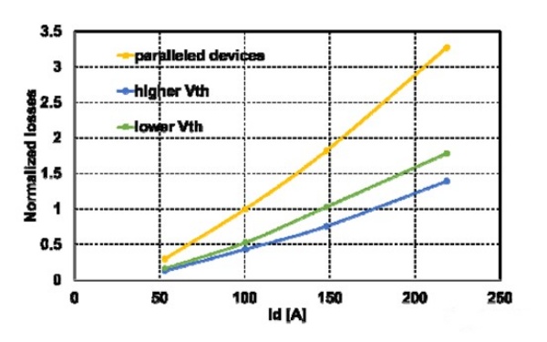
Similar to the positive temperature coefficient of on-resistance of silicon MOSFET, the same is true for silicon carbide MOSFET. Therefore, the higher the temperature, the greater the on-resistance and the smaller the current it carries. This characteristic hinders imbalance. Devices that originally bear more current due to the unbalanced Rdson will increase the impedance due to the increase in temperature, thereby reducing the current they bear, so this is a good aspect.
The second factor causing current imbalance is the conduction threshold voltage VGS-th of the silicon carbide MOSFET. If the conduction thresholds of two devices connected in parallel are different, for the same drive signal, the device with the smaller conduction threshold will be turned on first. , and when turned off, this device turns off later, which causes loss or energy imbalance on different devices connected in parallel.
In fact, the VGS-th parameter has a negative temperature coefficient as it changes with temperature. That is to say, the higher the temperature, the lower the conduction threshold. Therefore, one of the devices is too hot due to a different VGS-th. Over time, During operation, the corresponding VGS-th of this hot device will be lower, so the switching time will be longer and it will become hotter, which is a negative aspect for imbalance. Therefore, if the VGS-th difference is large at light load or in applications dominated by switching losses, thermal runaway is particularly likely to occur.

From Figure 2 above, you can see that two 1200V, 50A high-voltage silicon carbide connected in parallel will produce a large turn-off loss due to a certain VGS-th difference (700mV). The conduction loss difference caused by the difference in VGS-th has a small impact. Because of the positive temperature coefficient factor of Rds-on itself, this part of the loss difference can be compensated to a certain extent.
The third aspect that causes unbalance is mainly the driving circuit factors. Generally, in order to reduce switching losses, it is hoped to switch devices at the fastest speed, but the gate-level oscillation problem must also be considered. The gate-level driving resistance Rg and The way the lines are driven is very important to these problems.

Gate-level drive circuits generally have the above recommended methods, [sensitive words] a method of sharing gate-level resistors, without considering other uneven current balancing factors (such as Rds-on, VGS-th, etc.), the drive signal Arrive at the same time, so current sharing is easy, but the RLC resonance generated by the shared drive resistor is prone to gate-level oscillation. In the second method, due to the use of separate gate-level drive resistors, gate-level oscillation is less likely to occur, but due to resistance differences, current imbalance is likely to occur. Therefore, the more recommended method is to use the third method, which has both shared gate-level resistors and separate drive resistors. Combining the [sensitive word] and second methods can achieve better results.
The fourth factor that affects parallel balance is mainly the imbalance of source and drain parasitic inductance caused by layout. As shown in Figure 4, Ld and Ls are the parasitic inductances of the device drain and source respectively.
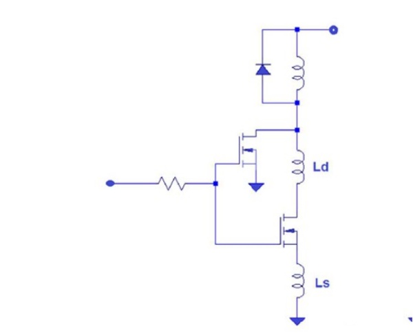
Among them, the Ls parasitic inductance, that is, the unbalanced source parasitic inductance, is the main factor causing the unbalanced current of parallel devices, while the drain inductance has a relatively large impact on the drain voltage stress, which is not within the scope of our discussion this time. Therefore, it is generally recommended to design the source traces as symmetrically as possible to make the source parasitic inductance symmetrical, or reduce its mismatch to avoid current imbalance.
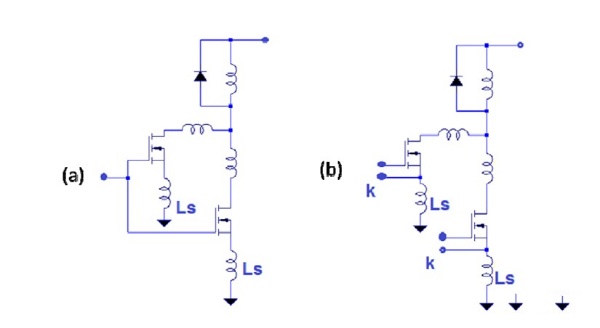
When the device switches, the voltage generated by the larger di/dt on the source parasitic inductance Ls will be fed back to the gate drive circuit. Therefore, when a separate source connection is not used as shown in Figure 5, b, there will be The imbalance of the source voltage will produce additional switching losses and will also lead to a certain gate-level oscillation voltage. When a separate source connection is adopted as shown in Figure 5, b, the influence of the Ls feedback voltage does not need to be considered, and the driving signal will not be added to the source parasitic inductance.
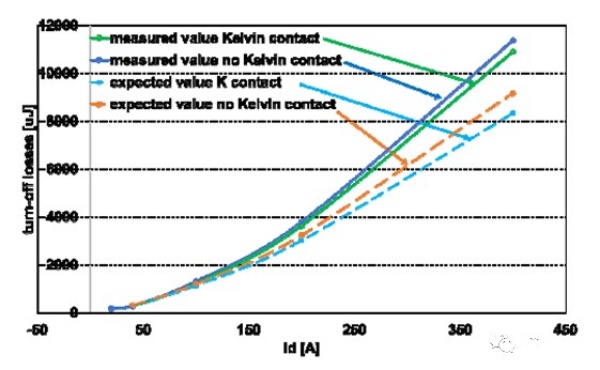
From the graph shown in Figure 6, we can see that when switching losses dominate, the sum of the turn-off losses of a single non-parallel device is smaller than the total turn-off loss of the two devices in parallel. In this sense, the switching loss When it dominates, parallel connection has little significance in reducing losses, but it can effectively average heat distribution. After the above analysis, we can know that when switching losses dominate, since there is no balancing effect of the positive temperature coefficient of Rds-on, if a current imbalance occurs, thermal runaway will easily occur.

If conditions permit, if there is no separate source driver connection, a 1ohm series resistor can be added to the source of the parallel device to achieve dynamic current sharing, which can reduce the di/dt of large drain currents and gate-level The series resistor RGoff can improve the parasitic oscillation caused by the unbalanced parasitic inductance of the source.
V. Parasitic turn-on effect of silicon carbide MOSFET and improvement measures
In the previous article, we also briefly analyzed the general requirements for gate-level drive waveforms of silicon carbide MOSFETs with a half-bridge structure. We will consider using negative voltage for reliable turn-off to avoid the impact of a smaller gate-level conduction threshold. And some unexpected gate-level coupling peak voltages cause false turn-on. However, the negative voltage withstand specifications of silicon carbide MOSFETs are not as large as those of silicon MOSFETs, so the specifications need to be strictly followed and a certain margin considered. Regarding the implementation of specific positive/negative voltage drive, there are many methods to achieve it, such as multi-channel isolated DC/DC power supply, or isolated driver IC with isolated DC/DC, etc.
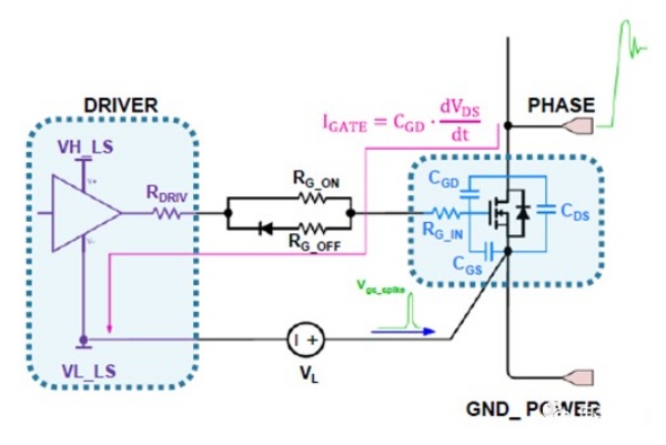
In fact, in the typical bridge circuit topology used in high-power circuits, the half-bridge structure is the basic topological unit, as shown in Figure 8. When the upper tube is turned on, that is, when the lower tube is turned off, the switching node generates a relatively large amount of energy. Large dV/dT, so this voltage will be coupled to a voltage pulse at the gate level through the silicon carbide parasitic capacitance CGD. Once this voltage pulse exceeds the gate turn-on threshold VGS-th value of the MOSFET, a false turn-on will occur, and we know that VGS -th is a negative temperature coefficient change. The higher the temperature, the lower the threshold, so this will be worsened at high temperatures. Once the lower tube is turned on by mistake, a short-circuit of the upper and lower tubes will inevitably occur, resulting in increased losses.
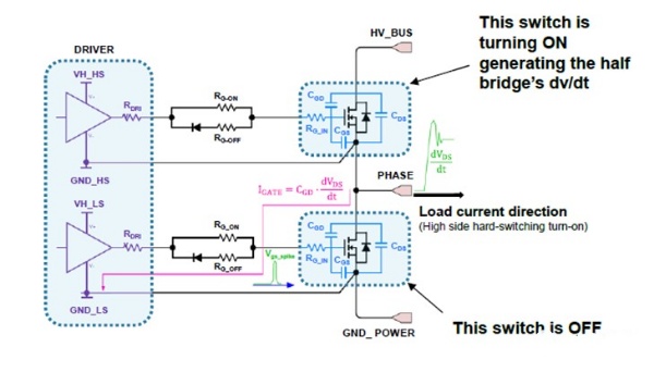
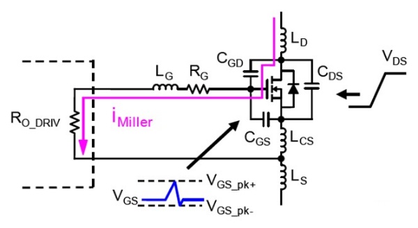
There are two situations for the gate-level peak voltage. When the upper tube is turned on and the lower tube is turned off, the lower tube will have a rapid dV/dT from low to high. Therefore, as shown in Figure 9, the node voltage passes through the CGD capacitor. Miller charging current is generated, which in turn flows through the driver's output resistor to produce a positive transient voltage at the gate level, as shown in Figure 9.
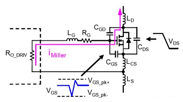
Another situation of gate-level spike is when the upper tube is turned off and the lower tube is turned on, the switching node generates dV/dT from high to low, so a reverse Miller charging current is generated, which then flows through the driver output. The resistor generates negative voltage spikes at the gate level. In this case, you need to pay attention to whether the negative voltage spike exceeds the negative voltage withstand voltage specification.
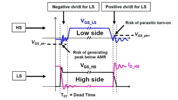
From Figure 11, we know that the gate-level oscillation before the low-side drive signal is turned on is mainly a negative voltage. This part of the voltage mainly considers the restrictions on the gate-level negative voltage specifications, while the gate-level oscillation after the low-side drive signal is turned off is mainly a positive voltage. this part of the voltage will mainly cause the half-bridge short circuit problem, so it needs to be considered.
We have clearly explained the reason why the parasitic effect is turned on, so what are the ways to suppress this effect? Generally speaking, the parasitic turn-on effect is caused by the large dV/dT of the drain, so limiting the change rate of dV/dT is a way to suppress the parasitic turn-on effect, but this conflicts with the goal of reducing switching losses.
In addition, regarding external factors, select a driver with a low pull-up resistance and set a low turn-off resistance RGoff, which allows the Miller current to pass through a lower impedance path and reduce the amplitude of the induced voltage. Of course, as mentioned in the previous article, if a negative voltage gate-level turn-off voltage is used, it can also effectively prevent the lower tube from accidentally turning on.
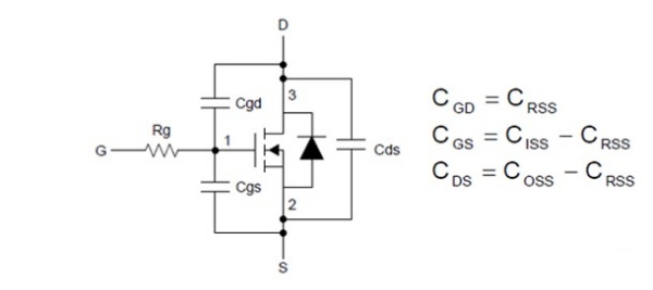
Make a fuss about the device itself, such as choosing a silicon carbide MOSFET whose CGS capacitance is much larger than the CGD capacitance. In this way, the current charging the gate-level capacitance through the Miller capacitance becomes weaker, as shown in Figure 13. Of course, you can also artificially A small capacitor is connected in parallel at the gate level to reduce the charging effect of the Miller capacitor on the gate-level capacitance, as shown in Figure 14, but it will also bring more switching and driving losses. Public data shows that under high-pressure applications, the ratio of CGS to CGD will be larger than under low-pressure applications, so it is more conducive to high-pressure applications.

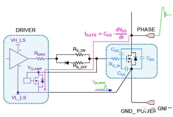
Another effective method is to use a Miller clamp circuit. When the gate voltage turn-off spike is detected, the Miller clamp circuit is turned on to clamp the gate voltage to GND, so that the Miller current will not pass through the driver output. The resistor raises the gate voltage, so that the silicon carbide MOSFET can be turned off using 0V voltage without using negative voltage to turn off. As shown in Figure 15, it is a VCLAMP circuit. Generally, this part of the circuit can be integrated into the driver chip.
VI. Considerations for short circuit protection of silicon carbide MOSFETs
An important parameter of silicon carbide MOSFET is short circuit withstand time (SCWT). Since this parameter involves device safety, it needs to be paid attention to. Due to the high current density of silicon carbide MOSFET, its chip occupies a small area, so its short-circuit withstand time is shorter than that of silicon MOSFET, so timely protection is required.
For a 1200V withstand voltage TO247 packaged silicon carbide MOSFET, under 700V conditions and 18V VGS driving voltage, its short-circuit withstand time is about 8-10uS. Turning off the silicon carbide MOSFET in such a short period of time will cause a very large dI/dT at the drain, resulting in a large drain voltage spike. In order to reduce the voltage spike, it is generally recommended to turn off the silicon carbide MOSFET slowly when a short circuit occurs and a large current occurs. cut off the VGS voltage.
In terms of specific implementation, sampling is generally performed through a current sampling resistor, and a desaturation action is performed on the short-circuited silicon carbide MOSFET. However, the disadvantage of this is that it causes additional losses, and the sampling circuit will increase the PCB space, so it is only used for Low power applications are shown in Figure 16. In high-power applications, the Vds voltage is generally used as the sampling voltage to trigger the overcurrent protection and desaturate the device. However, the accuracy of this method is not that high because the Vds obtained by Rdson sampling current has a certain range of variation, as shown in the figure 17 shown.
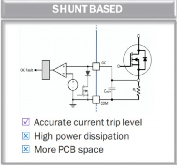
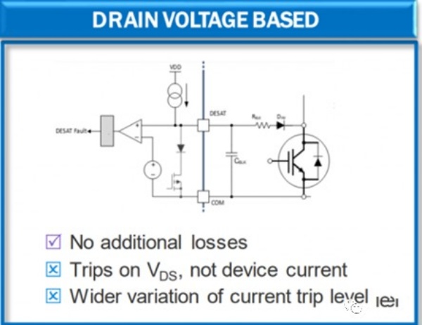
Using Vds sampling to design an overcurrent protection circuit is a very particular matter, because it is necessary to take into account both the timeliness of the trigger protection and the avoidance of false triggers. For the former, the worst case scenario of Rdson, as well as temperature and other factors need to be considered.
The typical detection desaturation time is generally around 250n-500nS when the signal is detected after the circuit is turned on, and it takes about 400n-1500nS to turn off the protection. In fact, it needs to be detected when saturation has not occurred (or the current has not yet been reached). before the peak value), you need to be able to detect the current signal, and cannot wait until saturation occurs before detecting the current signal.
VII. Considerations on silicon carbide MOSFET power device packaging
In high-voltage and high-power applications, plug-in packages such as TO220 or TO247 will be used. Therefore, during use, the length of the pins should be reduced as much as possible to reduce the parasitic inductance caused by the device packaging.
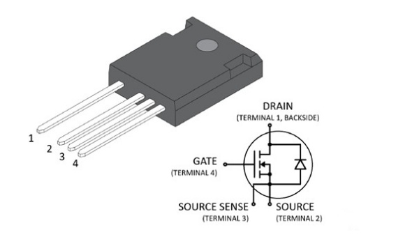
As discussed earlier in the parallel design of silicon carbide MOSFETs, wiring the MOSFET sources separately to the drive circuit will significantly reduce switching losses. The reason is that the source parasitic inductance will slow down the turn-on process or turn-off process and increase switching losses. Therefore, generally speaking, the TO247-4 package will have 30% less switching loss than the TO247 package.
To analyze this process specifically, we take the upper tube of the half-bridge as an example, as shown in Figure 18 (move Figure 8 here). When the switch is turned on, the current flows from top to bottom and gradually increases, then the source The induced voltage is positive on the upper side and negative on the lower side. This voltage will reduce the gate drive voltage, thus slowing down the turn-on process. Similarly, when the upper transistor is turned off, the current flows from top to bottom and gradually decreases, so the source induced voltage is positive below and negative above. This will increase the source drive voltage and therefore slow down the turn-off process. Both states will increase switching losses, so if switching losses dominate or are large, consider using TO247-4 packaging.

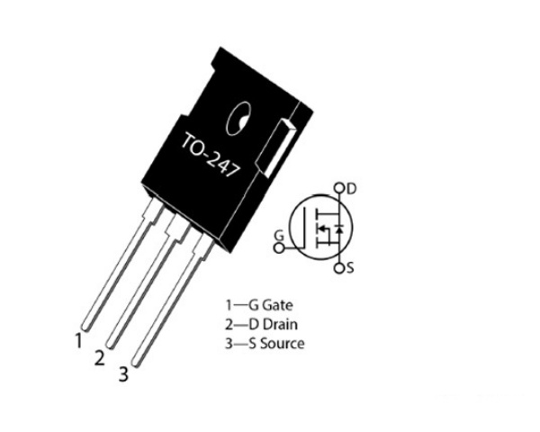
From the package diagram, as shown in Figure 19, the TO247-4 package has a separate source connection pin3, which is adjacent to the Gate pin to facilitate the application of drive signals, and the distance between the drain pin1 and the source pin2 is very small. Large, it needs to withstand the Vds high voltage. The pin arrangement of TO247 is relatively simple, with G gate, D drain and S source arranged in order.
In different packages of silicon carbide MOSFET modules, reasonable design to obtain smaller parasitic inductance is very helpful in limiting voltage overshoot, and at the same time, it will also increase the product's operating switching frequency as much as possible.
Through the discussion of the above seven parts, from the basic requirements of isolation drive, to the calculation of drive loss, from the parasitic turn-on effect of a single tube, to the implementation of multi-tube parallel connection, and the corresponding layout principles, several precautions are finally reminded from the packaging. I hope everyone can have a more thorough understanding of the silicon carbide MOSFET drive circuit so that it can be implemented in actual solutions to give full play to the performance of the silicon carbide MOSFET.
Comments
Post a Comment